
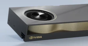


NVIDIA A100 Tensor Core GPU: Powering Next-Generation Data Center Intelligence
engineered for precision workloads demanding desktop-to-datacenter power
The evolution of artificial intelligence and high-performance computing hinges on a single technological bottleneck: processing power at scale. Enter the NVIDIA A100 Tensor Core GPU, a purpose-engineered accelerator that redefined what enterprise data centers can achieve. Unlike consumer-grade GPUs or entry-level compute accelerators, the A100 is architected from the ground up to handle the punishing demands of production AI workloads, large-scale simulations, and data-intensive analytics.
For organizations deploying cutting-edge machine learning models, training transformers on massive datasets, or running scientific computations that demand precision and speed, the A100 represents a quantum leap forward. This comprehensive guide explores the technical specifications, real-world deployment strategies, and competitive advantages that make the A100 the preferred choice for data center operators worldwide.


What Makes the NVIDIA A100 Tensor Core GPU a Data Center Game-Changer
The NVIDIA A100 Tensor Core GPU isn’t simply a faster version of its predecessors. It represents a fundamental reimagining of how GPUs can serve modern enterprise computing. Built on NVIDIA’s Ampere architecture and manufactured on TSMC’s advanced 7-nanometer process, the NVIDIA A100 delivers performance improvements that transcend incremental gains.
Consider the scope of the improvement: organizations leveraging the A100 report training times reduced from weeks to days or even hours. A model that might take seven days to train on legacy infrastructure can complete in less than 24 hours on A100 clusters. This isn’t merely a convenience but it fundamentally changes the economics of AI development, enabling faster experimentation cycles and reducing infrastructure costs per trained model.
The A100’s versatility is equally notable. A single GPU can dynamically partition into seven isolated GPU instances through Multi-Instance GPU (MIG) technology, meaning organizations can run multiple workloads simultaneously without performance contention. This elasticity appeals to enterprises with mixed AI workloads, research institutions balancing multiple projects, and cloud service providers optimizing utilization rates.
Technical Architecture: Understanding Tensor Core Performance
| Performance Metric | Peak Throughput |
|---|---|
| FP32 (Single-Precision) | 19.5 TFLOPS |
| TF32 (TensorFloat-32) | 156 TFLOPS |
| FP16/BF16 (Half-Precision) | 312 TFLOPS |
| FP16/BF16 with Sparsity | 624 TFLOPS |
| INT8 (8-bit Integer) | 624 TOPS |
| FP64 (Double-Precision) | 19.5 TFLOPS |
The NVIDIA A100’s computational power originates from its third-generation Tensor Cores which are specialized hardware units engineered exclusively for the matrix operations that power deep learning. These aren’t general-purpose computing cores; they’re laser-focused on the mathematical operations that drive neural networks.
This architectural flexibility means organizations can tailor compute precision to their specific workload requirements. Model training can leverage mixed-precision approaches that trade marginal accuracy for substantial speed gains. Scientific simulations requiring double-precision mathematics run efficiently without architectural compromises.
The performance jump relative to previous generations is substantial. The NVIDIA A100 Tensor Core GPU delivers up to 20× faster training than the Volta generation when using TF32 precision without requiring code modifications. For AI-specific workloads like BERT language model training, organizations observe roughly 1.95× performance acceleration compared to V100 GPUs while maintaining identical model accuracy.